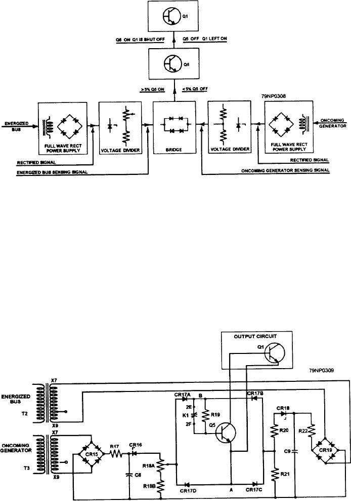
Figure 8-39.--Block diagram of voltage difference monitoring circuit.
voltage at T3. Transformer T3 steps the voltage down.
Producing and delivering a sensing signal from
CR15 rectifies it, and R17 and C8 filter it.
each input
Zener diode CR18 is used to increase the sensitivity
Comparing the difference in magnitude of the
of voltage dividers R20 and R21 in the bus signal circuit.
two sensing signals in a bridge circuit
The Zener diode causes all the increase or decrease of
Using transistor Q5 for an ON-OFF switch
the bus signal voltage to appear across the voltage
divider. This also happens to voltage dividers R18A and
Look at the schematic in figure 8-40. You can see
R18B, using Zener diode CR16. The resultant signal
that the bus voltage is stepped down by windings X7 and
out of each voltage divider is the sensing signal. These
X9 on T2. The reduced voltage is then rectified by a
sensing signals are then fed to a rectifier bridge
consisting of CRs 17A, B, C, and D. When the bus and
full-wave rectifier CR19 and filtered by R22 and C9.
the oncoming generator sensing signals are equal, there
The same thing occurs for the oncoming generator
Figure 8-40.--Schematic diagram of voltage difference monitoring circuit.
8-43

