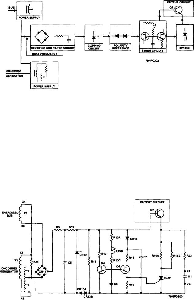
Figure 8-33.--Block diagram of frequency difference monitoring circuit.
3. The beat frequency voltage is clipped by resistor
(fig. 8-33). It rectifies, filters, and reduces the beat
frequency voltage. It then uses the beat frequency
R10 and Zener diode CR12 to a constant dc level
voltage in a timing circuit to fire an SCR.
(fig. 8-35, view D)
Look at the schematic in figure 8-34. The
4. The signal is now sent to resistor R11 and diode
secondary windings X4 and X6 of T2 and X4 and X6 of
CR13 (views A and B). Here, about 1 volt is
T3 are connected in such a manner that a beat frequency
subtracted from the clipped beat frequency
voltage (heterodyne wave) is generated. This beat fre-
signal (fig. 8-35, view E) to ensure the clipped
quency voltage is the difference between bus and oncom-
beat frequency voltage signal goes to zero when
ing generator frequencies (fig. 8-35, view A). Refer to
the original beat frequency goes to zero
figures 8-34 and 8-35 as you see how the circuit functions:
5. The clipped beat frequency voltage signal is
1. The beat frequency voltage is rectified by CR11
applied across base 1 and base 2 of unijunction
transistors Q3 and Q4 (fig. 8-34). This signal is
2. The resulting dc signal (fig. 8-35, view B) is
also applied to the RC circuit, consisting of
filtered by resistor R9 and capacitor C5 (fig.
resistors R13A, R13B, R13C, and capacitor C6.
8-35, view C)
Figure 8-34.--Schematic diagram of frequency difference monitoring circuit.
8-40

