Biasing for the second amplifier is such that it
DECELERATION MODE.-- With the external
switch or contacts (connected to TB1 terminals 14 and
operates as a saturation switch. The negative trigger
15) open, the positive voltage from A3A1R1 forward
spikes saturate Q3 and hold Q3 saturated until the spike
biases current switch A3A1Q1. With Q1 turned on, -9
decays sufficiently below the threshold voltage to turn
volts are connected through Q1 to LOW SPEED
Q3 off. This produces a pulsed output with the
potentiometer A3R1. The LOW SPEED potentiometer
frequency determined by the engine speed and the pulse
sets the amount of negative speed-setting bias voltage
width determined by the selected time constant. Zener
to hold the prime mover at the desired idle speed.
diode A4A1VR1 clamps the maximum pulse excursion
A C C E L E R A T I O N M O D E . -- Closing the
to 6.6 volts.
external ramp switch or contacts connected to TB1
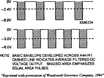
As the engine rpm increases, so does the frequency
terminals 14 and 15 connects -9 volts dc to timing
of the speed input signal (see fig. 9-19). The value of
capacitor A1C1 and current switch A3A1Q1. This
capacitance selected sets the speed range of the speed
reverse biases Q1 and stops the current flow through Q1.
sensor to match the requirements of the engine. Higher
This allows the right side of C1 to charge from -9 volt
rpm engines require a faster differentiator network time
dc toward +9 volt dc his positive ramp voltage is
constant. This maintains the proper ratio between the
applied through gate diode A3A1CR2 to the amplifier
summing point. ACCEL potentiometer A3R2 sets the
pulse width and the puke period (time between pulses).
charge time constant of the circuit, thereby setting the
The output from second amplifier Q3 is filtered by
acceleration rate of the ramp generator. The ramping
a two stage RC filter consisting of R4/C2 and R5/C3.
output voltage continues in a positive direction until it
For all practical purposes, the filtered output voltage is
reaches 0 volt dc As the ramp becomes more positive
proportional to the engine speed (see fig. 9-19). If the
than 0 volt dc, gate diode A3A1CR1 forward biases and
engine speed decreases, the frequency of the
begins to conduct. This clamps the ramp generator
differentiated spikes decreases. This increases the time
output to +0.6 volt dc At this time the prime mover
should be at or near rated speed and the reference
between pukes. Since the pulse width is determined by
voltage at the summing point will be 0 volt dc.
the differentiator time constant, the pulse width remains
the same. This decreases the average dc voltage level
from the filter circuit.
Speed Sensor
During normal operation the clipped sine wave
output signal from the first amplifier is coupled through
The speed input signal from the magnetic pickup is
gate diode A4A1CR4 and charges integrating capacitor
applied to interstage transformer A4T1 (see fig. 9-18).
C1. When C1 charges sufficiently negative, fail-safe
Transformer T1 provides a 1 to 3 step-up ratio of the
transistor Q4 turns on and saturates. This clamps the
speed input signal. The alternating input signal from T1
alternately drives first amplifier A4A1Q1/Q2 into
anode of VR2 at the dc common potential. In this mode
saturation and cutoff. This clipped sine wave output
the negative fail-safe supply voltage, which is connected
signal is applied to the selectable time constant
through the fail-safe jumper, is dropped across R7.
differentiator network.
Differentiator networks A4C1/A4A1R9 and R12
convert the clipped sine wave from the first amplifier to
corresponding positive- and negative-going spikes.
Capacitor A4C1 is selectable to set the proper time
constant for the particular engine speed for which the
2301 electric control is used. The value of capacitance
selected determines the decay time of the positive and
negative spikes.
The positive- and negative-going spikes are applied
to gate diode A4A1CR3. The gate diode passes only the
negative-going spikes and rejects the positive spikes.
These negative spikes trigger the second amplifier
Figure 9-19.--Speed sensor output voltage.
A4A1Q3.
9-27

