pin packages (SIPPs). Memory pcb’s also operate on a
request basis, but unlike memory modules, there is not
a priority sequence to go through. The request is made
by requestor, the control circuitry selects either a read
or a write operation, and the timing circuitry initiates
the read and/or write operations.
Memory Architecture
The memory architecture, regardless of the
memory type, is consistent. Memories are typically
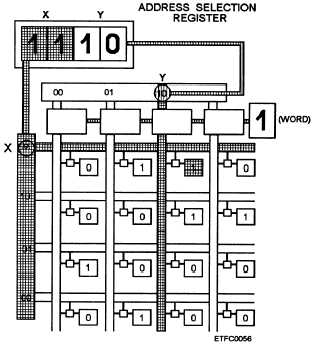
organized in square form so they have an equal number
of rows (x) and columns (y) (fig. 6-4). Each intersection
of a row and column comprises a memory word
address. Each memory address contains a memory
word. The selected memory address can contain one
or more bits. But for speed and practicality, for a given
computer design, the word size typically relates to the
CPU and is usually the size of its registers in bits. Word
sizes typically range in increments of 8, 16, 32, or 64
bits. Figure 6-5 represents an address with an 8-bit
word. The methods used for the arrangement of the
rows and columns vary in a given type of memory. The
rows and columns are arranged in arrays, memory
planes, or matrices.
MEMORY OPERATIONS
Memories operate on a request, selection, and
initiate basis. A memory request or selection and a
memory word location are transmitted from the
Figure 6-4.—Row (X), column (Y) organization.
requestor (CPU or I/O sections) to the memory section.
The computer’s internal bus system transmits the
memory request or selection and location to the
memory section. The memory operations, regardless of
the computer type, share some basic commonalities.
Key events must occur to access and store data in
memory. Some items only occur with certain types of
memories, and we discuss these as you study each
different type of memory. We also discuss the items that
are common to most memories: control circuits,
timing circuits, and memory cycle. In addition, we
present methods used for detecting faults and
protecting memory.
Memory Interface Circuits
The memory interface circuits include all the lines
of communication (buses) and the interfacing register
between the requester (CPU or I/O(C)) and memory.
The communications lines include some of the
following:
Data (bidirectional bus)
Control lines (write byte and interleave [for large
computers])
Memory request
Read and write enables
Data ready
Data available
The interface (data) register (often designated as
the “Z” register) functions as the primary interfacing
component of memory. Before the read/write
operation, this register transfers the selected memory
address to the address register. All data entering and
leaving the memory is temporarily held in this data
register. In a write operation, this register receives data
from the requester; and in a read operation, this register
transmits data to the requester. For computers with
destructive readout, it routes the data back to memory
to be rewritten.
Control Circuits
The control circuits set up the signals necessary to
control the flow of data and address words in and out of
memory. They screen the request or selection by units
external to memory—the CPU and/or IO(C).
Depending on the computer type, some of the more
common uses of the control circuits include:
6-4


