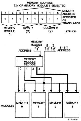
For our second example, refer to figure 6-7. It
shows an 8-bit memory address, a memory module
decoder, and four memory modules (each with l008
addresses). In the figure, the memory address register
or translator contains 3728. When a memory reference
takes place, the address translation logic decodes the
two most significant bits of the 8-bit logical address to
determine and select the applicable memory module.
The lower six bits of the logical address are passed to
all the memory modules to determine the row (x) and
column (y) intersection, but only the selected memory
module decodes the address. In this example, memory
address 728 of memory module 3 is addressed. This
means a word will be read from (or written into) this
address. The following is a breakdown of the address:
Figure 6-7.—8-bit address with memory module.
READ CYCLE.— Processing a read request
requires memory to read data from the addressed
memory location and transmit the data via a bus to the
requesting section of the computer where it is used for
calculations or output to another device. The
information read
program, general
from memory can be part of a
data, calculations, or operands.
Remember, information read from a destructive readout
memory has to be written back into memory or it will
be lost. Also remember, for some memory types, read
and write operations are separate. Depending on the
computer’s instruction set, the information can be read
from anywhere in memory or any part of a memory
address.
WRITE CYCLE.— A write request, on the other
hand, causes memory to accept information from a bus
and to store (write) the information in the addressed
memory location. Again the information can be part of
a program, data, calculations, or an operand. The
information can come from the CPU or another device.
For those memories that are destructive, the write cycle
is a must to retain the original data after a read.
Otherwise, it is a separate operation. Just as in a read
cycle, the computer’s instruction set allows the
information to be written into any memory address or
part of a memory address in a read/write memory.
INTERLEAVE.— A large memory may be
organized in several modules, each covering a portion
of the addressable space. The effective speed of this
memory can be increased if memory access cycles in
different modules are overlapped. In such a system, the
CPU requests a read or write operation in one module.
Then, it requests other memory operations in other
modules before the result from the first module
becomes available. Because program instructions are
usually fetched from successive locations in the main
memory, overlapped operation may be achieved by
arranging memory addresses such that successive
addresses refer to different modules. For example, if
there are four modules, the first module should contain
words 0, 4, 8, . . . etc; the second module words
1, 5, 9, . . . etc; and so on. The increase in speed with
memory interleaving is achieved at the expense of
increased complexity in the CPU and memory control
circuitry.
Memory Fault Detection
A variety of methods is used to ensure the accuracy
of data written into and read from the memory section.
The methods include parity check and error bit
detection and/or correction.
PARITY CHECK.— Parity check is one of the
simplest methods used to detect read/write errors in core
memory. The strategy is simple; the computer counts
the number of ones in a memory word, then adds an
extra bit to make the total number of ones either an even
number or an odd number depending on whether the
6-7


